- [ previous ] -
[ top ] -
[ next ] -
5.1 VTX R&Ds
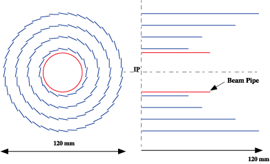
 Present Baseline Design ; four layers at r = 24, 36, 48, 60mm
. . . This layout could be too simple and beautiful.
Requirements and R&D items
- Position resolution be better than 4miron
. . . Already 3micron achieved by testbeam measurement.
- Innermost layer as close to IP as possible
. . . r = 24mm may be too large : r = 15mm at CDF SVX-L00.
- Extremely-thin CCD (toward 20micron) and its Distortion
- Room-temperature operation
- Radiation hardness
- 3-years life-time at so-far-standard luminosity. --> What about High-Lum mode ?
- Notched Structure / Fat-Zero Charge Injection / Fast Readout / Optimized temperature
- Electron-beam irradiation in JFY2002 for precise prediction of damage.

- Fast (40MHz) Readout
- for better Radiation Hardness
- to reduce Readout Channels
- Module Design/Production in progress

 See HwanBae-san's talk for detail.
yoshiaki.fujii@kek.jp, July 10,2002 at 5th ACFA LCWS at Tokyo


 Present Baseline Design ; four layers at r = 24, 36, 48, 60mm